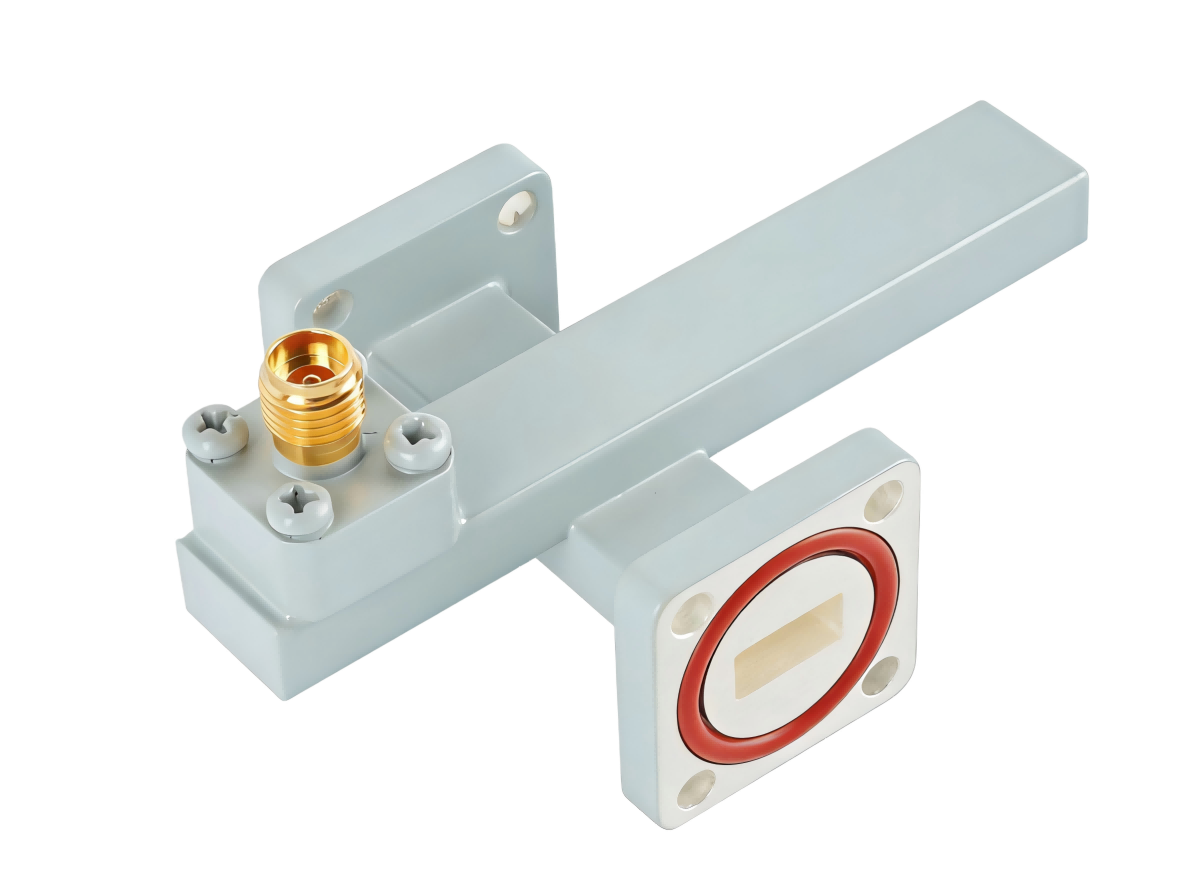
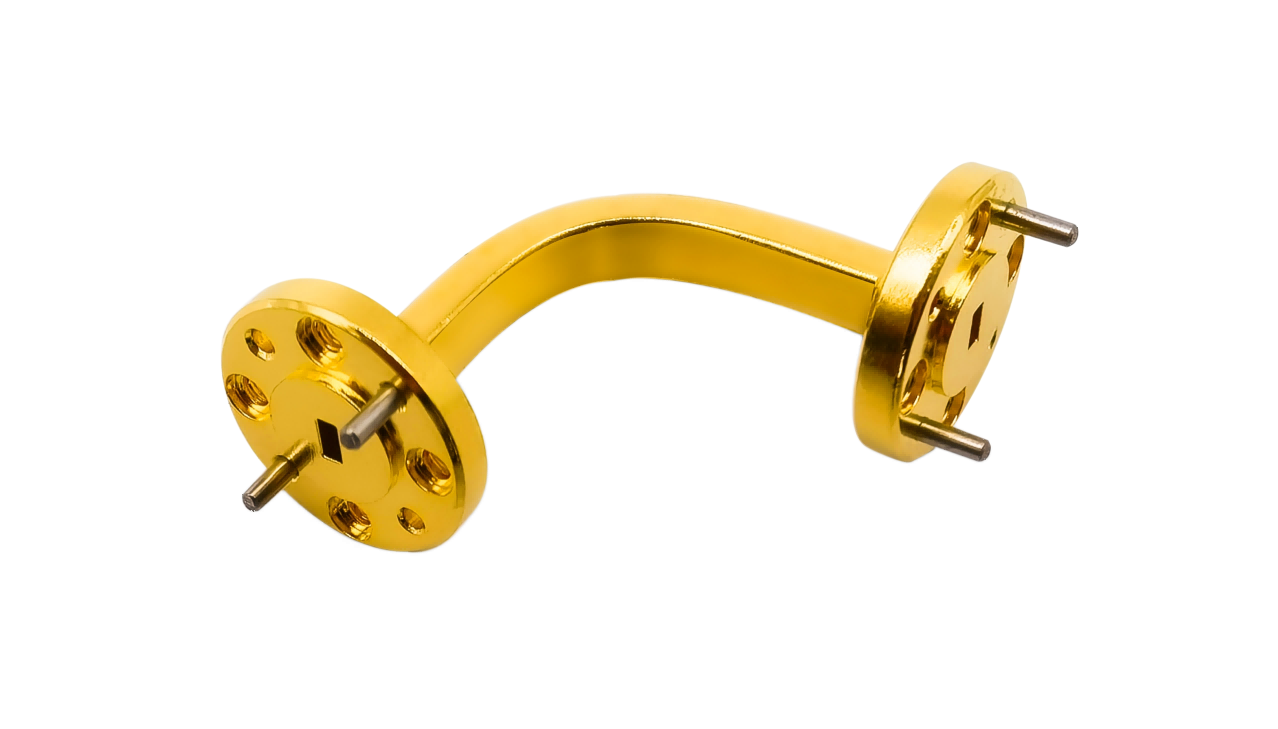
Waveguide E-Bend
Waveguide E-Bend components allow efficient signal routing in the E-plane while maintaining low insertion loss and high power handling. Widely used in microwave transmission systems, radar platforms, satellite communication equipment and RF laboratory setups.
High-Precision Waveguide E-Bends for Compact RF Routing
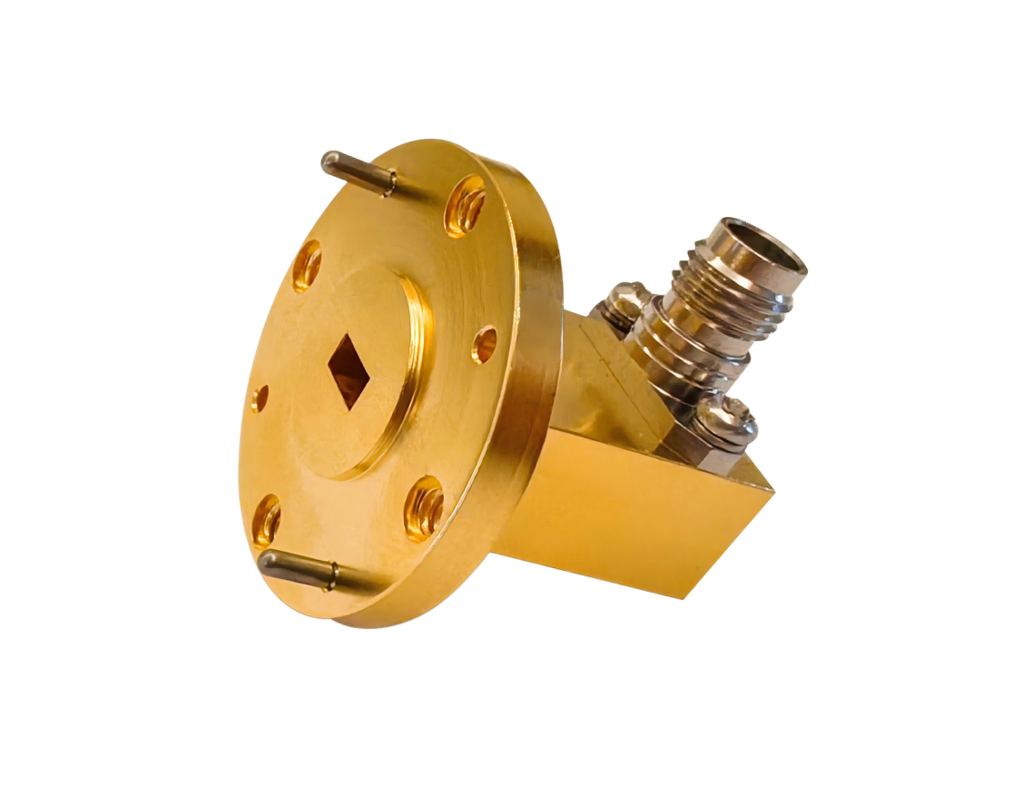
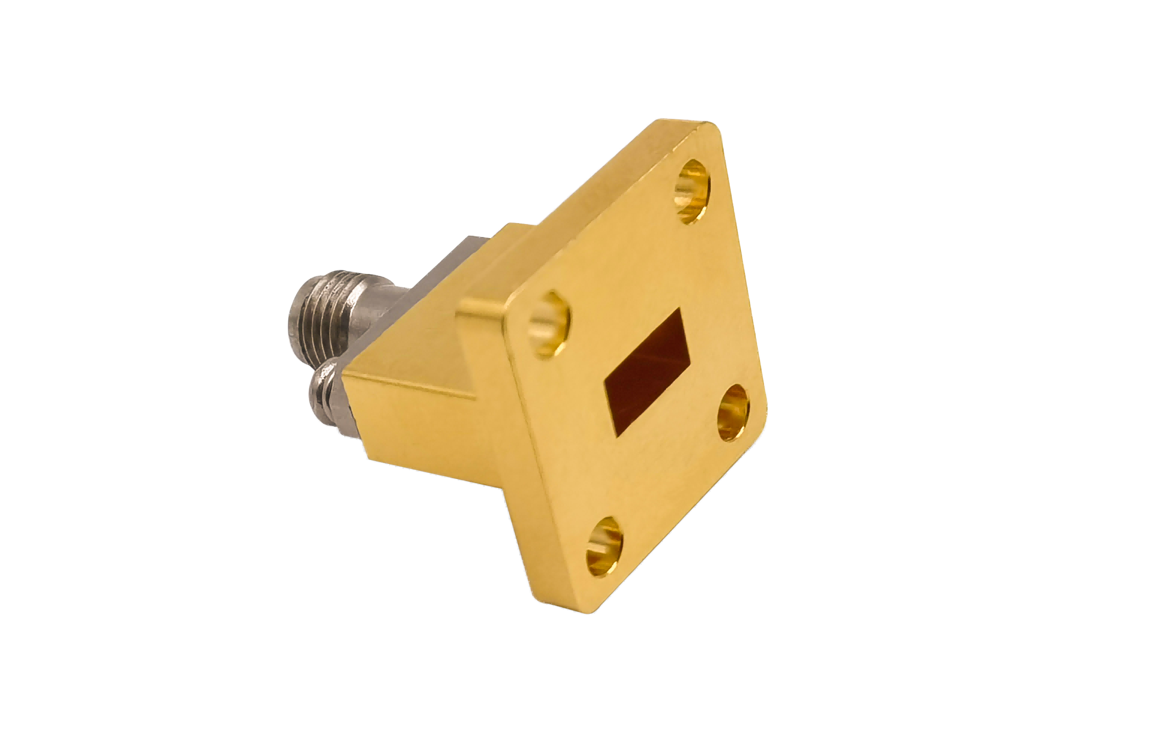
AO Microwave's waveguide E-bends (Electric-plane bends) are engineered to alter signal propagation paths along the narrow wall of rectangular waveguides. Precision-manufactured to support frequencies up to 110 GHz, our E-bends maintain a low typical VSWR of < 1.10:1 (with select models achieving < 1.05:1 in optimized bands). By utilizing precise machining techniques, we minimize phase distortion and reflections at standard 90° and 45° bend angles, offering dependable routing components for high-density radar feeds, airborne systems, and millimeter-wave instrumentation.
To ensure reliable long-term mechanical strength and consistent electrical conductivity, our E-bends are fabricated from high-grade metals with advanced surface protection:
- Aluminum: The preferred material for lightweight structural requirements, frequently utilized in airborne and aerospace payloads.
- Copper: Selected for high-power layouts demanding minimum RF attenuation and optimized thermal performance.
- Stainless Steel: Available for specialized cryogenic testing or highly corrosive setups requiring thermal isolation.
- Surface Finishing: High-purity silver plating for minimized skin-effect attenuation, gold plating for oxidation prevention, chemical passivation, and weather-resistant paint.
| Part No | Frequency/GHz | VSWR (Max) | IL/dB (Max) | Standard Length/mm | Flange Type |
|---|---|---|---|---|---|
| AO430-WEBAXBPPACG | 1.72-2.61 | 1.1 | 0.2 | A=150 B=150 | UDR22 |
| AO340-WEBAXBPPACG | 2.17-3.30 | 1.1 | 0.2 | A=100 B=100 | UDR26 |
| AO284-WEBAXBPPACG | 2.60-3.95 | 1.1 | 0.2 | A=100 B=100 | UDR32 |
| AO229-WEBAXBPPACG | 3.22-4.90 | 1.1 | 0.2 | A=80 B=80 | UDR40 |
| AO187-WEBAXBPPACG | 3.94-5.99 | 1.1 | 0.2 | A=80 B=80 | UDR48 |
| AO159-WEBAXBPPACG | 4.64-7.05 | 1.1 | 0.2 | A=80 B=80 | UDR58 |
| AO137-WEBAXBPPCSG | 5.38-8.17 | 1.1 | 0.3 | A=70 B=70 | UDR70 |
| AO112-WEBAXBPPCSG | 6.57-9.99 | 1.1 | 0.3 | A=50 B=50 | UBR84 |
| AO90-WEBAXBPPCSG | 8.20-12.5 | 1.1 | 0.3 | A=40 B=40 | UBR100 |
| AO75-WEBAXBPPCSG | 9.84-15.0 | 1.1 | 0.3 | A=40 B=40 | UBR120 |
| AO62-WEBAXBPPCSG | 11.9-18.0 | 1.1 | 0.3 | A=40 B=40 | UBR140 |
| AO51-WEBAXBPPCSG | 14.5-22.0 | 1.1 | 0.3 | A=30 B=30 | UBR180 |
| AO42-WEBAXBPPCSG | 17.6-26.7 | 1.1 | 0.3 | A=30 B=30 | UBR220 |
| AO34-WEBAXBPPCSG | 21.7-33.0 | 1.1 | 0.3 | A=30 B=30 | UBR260 |
| AO28-WEBAXBPPCSG | 26.5-40.0 | 1.1 | 0.3 | A=30 B=30 | UBR320 |
| AO22-WEBAXBPPCG | 33.0-50.0 | 1.15 | 0.5 | A=25 B=25 | UG-383/U |
| AO19-WEBAXBPPCG | 40.0-60.0 | 1.15 | 0.5 | A=25 B=25 | UG383/UM |
| AO15-WEBAXBPPCG | 50.0-75.0 | 1.15 | 0.5 | A=25 B=25 | UG385/U |
| AO12-WEBAXBPPCG | 60.0-90.0 | 1.15 | 0.5 | A=25 B=25 | UG-387/U |
| AO10-WEBAXBPPCG | 75.0-110.0 | 1.15 | 0.5 | A=25 B=25 | UG387/UM |
Waveguide E-Bend Engineering Considerations
An E-bend redirects electromagnetic waves along the direction of the E-field. When designing systems with E-plane routing, engineers must select the correct bend geometry to match system envelope and power budgets:
1. Sweep Radius vs. Mitered Designs
Sweep (Radius) E-Bends feature smooth internal curvatures, offering broad operating bandwidth and low insertion loss. For space-restricted enclosures, Mitered E-Bends utilize a precise, calculated 45-degree internal reflective corner to achieve an ultra-compact 90-degree turn, though over a slightly more constrained frequency band.
2. Minimizing RF Breakdown (Arcing)
Since E-bends alter the narrow wall of the rectangular waveguide, they naturally concentrate the electric field at the inner bend corner. In high-power transmitter systems, sharp internal edges or imperfections can cause RF voltage breakdown. Precision inner profiling is required to keep electric field stress well below ionization thresholds.
Overcoming Critical E-Bend Design Challenges
We address the common mechanical and electrical issues frequently discussed by engineers on hardware forums:
Preventing Tube Deformation & Wrinkling during Bending
Bending raw waveguide tubing along its narrow wall puts extreme tension on the outer wall (causing thinning) and high compression on the inner wall (causing wrinkling). Physical deformation distorts the internal rectangular dimensions, leading to high reflection. We utilize precision CNC-controlled bending mandrels and split-block machining to guarantee uniform inner dimensions and a smooth internal finish, preventing VSWR degradation.
Managing Phase and Amplitude Matching
In multi-port radar feed networks or monopulse comparators, any physical path-length deviation in the E-bend alters phase matching between channels. Our production lines utilize automated coordinate measuring machines (CMM) to ensure dimensional repeatability of ±0.03 mm, enabling consistent phase and amplitude balance across multiple units.
Where Waveguide E-Bends are Deployed
Our precision E-bends are integral to dense microwave plumbing where vertical routing is necessary:
- Airborne & Fighter Radar Feeds: Lightweight aluminum E-bends designed to fit inside extremely tight aircraft nose cones.
- Satellite Payload Assemblies: High-performance routing segments subjected to vacuum environments, requiring low-outgassing characteristics and strict thermal stability.
- Millimeter-Wave (mmWave) Transceivers: Standard components in 5G/6G prototype backhauls and high-frequency instrumentation testing.
Waveguide E-Bend FAQs
Need high-precision Waveguide E-Bends?
Specify your WR size, bend angle (90°/45°), radius type, and flange — we'll quote in 24 hours.